High-throughput experimental screening of oxide semiconductor materials
Zongkai Yan1, Panfeng Zhao1, Yilan Pan1, Jun Zhu2, Yong Xiang1*
1 School of Materials and Energy, University of Electronic Science and Technology of China, Chengdu, 611731, China
2 School of Electronic Science and Engineering, University of Electronic Science and Technology of China, Chengdu, 611731, China
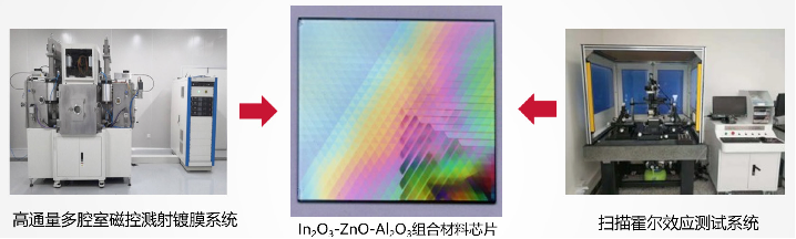
EXTENDED ABSTRACT: OLED display is one of the emerging strategic industries in China. Generally, the performance of OLED displays is determined by the operating frequency of thin film transistors (TFT), which depends on the semiconductor material of the channel layer. To support the development of high-generation lines and ultra-high-definition (8K × 4 K) display technology in the future, large-area thin films are required to be prepared with high uniformity, while the carrier mobility of the channel layer material should be larger than 40 cm2 /Vs. Amorphous oxide semiconductor (AOS) is one of the current mainstream technology routes for the channel layer. It has the characteristics of being suitable for large-area preparation, low production cost, and simple preparation process, and is especially suitable for the application of high-generation lines. However, there are two major technical bottlenecks in the application of this material. One is the lower carrier mobility compared with the low temperature polysilicon (LTPS) and needs to be further improved; The other is the potential segregation of compositions and structures during the large-scale production, resulting in a decline in production yield. Therefore, it is necessary to develop a process technology with a wider process parameters window to ensure that both high volume and yield are achieved at the same time. The high carrier mobility of the AOS could be attributed to the overlap of the spherically symmetric ns (n>5) electron orbitals in the Indium ion and other metal ions, enabling relatively high carrier mobility even for its amorphous form. In order to realize the regulation of its carrier mobility and carrier concentration, elements replacement and process optimization are required. Moreover, it is necessary for further studies on the different preparation process parameters of the various material compositions. In the previous research, high-throughput experimental research was carried out on the InZnO-based amorphous oxide semiconductor material through the combinatorial magnetron sputtering technology and the micro-area Hall effect characterization technology, which screened out some new amorphous oxide semiconductor materials with higher carrier mobility, moderate carrier concentration and wide process window. Based on the previous results, the reporter is willing to discuss the application of high-throughput experimental technology related to oxide semiconductor materials.
REFERENCES
[1] Burger, B., et al. A mobile robotic chemist. Nature, 2020, 583, 237-24.
[2] Yan, Z., et al. Rev. Sci. Instrum. 2020, 91, 065107.
Zongkai Yan obtained his Ph.D. degree in Materials Science from University of Electronic Science and Technology of China in 2018. Currently, he is a XX in the School of Materials and Energy, University of Electronic Science and Technology of China. His research is focused on Material Genome Engineering, especially high-throughput experiments. He has published more than 10 papers in reputed journals, such as Applied Surface Science, Review of Scientific Instruments, ACS AMI, etc.