The preparation and characterization of two-dimensional materials
Zegao Wang
College of Materials Science and Engineering, Sichuan University, Chengdu, China
EXTENDED ABSTRACT: Recently, 2D layered semiconductors have brought new possibility for the applications in electronics and photo-electronics. Compare to traditional semiconductor, the intrinsic dark current is lower which enable to realize the photodetection at room temperature. The large range of the band gap also facilitates to fabrication 2D materials based photodetector covering from the visible light to infrared light, even to long-wavelength infrared. However, currently, their electronic properties are low limiting their real application, for example the carrier mobility are usually much lower than that of graphene. In addition, the low light adsorption of two dimensional also influence its photodetection. Understanding origins of the light-matter interaction is of great importance to the rational design of highly efficient photodetection. In this talk, we will introduce our recent study, including the materials growth, structure analysis and device investigation. We will firstly introduce our recent fabrication of the p-type 2D semiconductor. Through controlling the fabrication, the large-scale PtS film has been synthesized and demonstrated showing a p-type behavior from studying its transfer curves in transistor, Schottky contact property, et al. Besides, the heteroatoms doping in 2D materials, such as Nb and V et al, will also been discussed. It has been demonstrated that the heteroatom doping would change the electrical property of MoS2 exhibiting the p-type doping effect. Then, we will introduce the interface investigation by using the scanning probe techniques, which revel the electrical property of the 2D materials in nanoscale. The build-in electric filed in PtS/MoS2 p-n heterojunction and Nb-MoS2/MoS2 homojunction will be discussed. At last, the tunable photoelectrical property including the photoresponse, detectivity and rise/fall time has been studied. The results show that by applying the external electric filed, it was able to tune the light-matter interaction resulting in tunable photodetection, where the photoresponse could be tuned up to 50 A/W, and the detection range could extend from visible to near infrared.
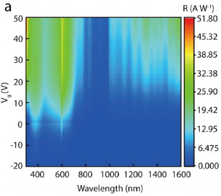
Figure 1. The photoresponse of 2D materials.
REFERENCES
[1] Zegao Wang*, et al. Adv. Funct. Mater., 2021, 10.1002/adfm.202104367.
[2] Zegao Wang*, et al. Mater. Today Phys., 2021, 16, 100290.
[3] Zegao Wang*, et al. ACS Nano, 2021, 15, 13279.
[4] Zegao Wang*, et al. ACS Appl. Mater. Interfaces, 2020, 12, 49830.
[5] Zegao Wang, et al. Nature Commun., 2021, 12, 1709.

Prof. Dr. Zegao Wang was got his Ph.D. degree from University of Electronic Science and Technology of China under the supervisor from academician member Prof. Yanrong Li in 2014. Then he was employed as postdoctoral in Aarhus University in Prof. Mingdong Dong’s group. In 2018, he was joined in Sichuan University as a professor. Dr. Zegao Wang’s research focus on the synthesis and property of two dimensional electronics materials including graphene, MoS2, PtSe2 et al. Especially, he focusses on developing new mythology to in-situ study the local transport mechanism by scanning probe technology. Until now, he has published more than 150 papers, including Advanced Materials, Science Advances, Nature Communications et al, and has been serving as a young editorial board member of Chinese Chemical Letters, and International Journal of Minerals, Metallurgy and Materials.